Charge Coupled Devices belong to integrated circuits, which are neatly arranged with many capacitors, which can sense light and convert images into digital signals. Through the control of an electric circuit, each small capacitor can transfer its charge to its adjacent capacitor. CCD is widely used in digital photography, astronomy, especially photometry, optical and spectrum telescope, and high-speed photography techniques such as nebula imaging.

The Development of CCD technology
The CCD was invented in 1969 by Willard Sterling Boyle and George Elwood Smith of Bell Labs in the United States. Bell Labs was developing video phones and semiconductor bubble memory at that time. Combining these two new technologies, Boyle and Smith came up with a device named Charge “Bubble” Device.
The characteristic of this device is that it can transfer charge along the surface of a semiconductor, so it tries to use it as a memory device. At that time, memory could only be “injected” from the register. However, it was immediately found that the photoelectric effect can generate electricity on the surface of this component and form a digital image.
In 1971, researchers at Bell Labs were able to capture the images with simple linear devices, and CCD was born. Several companies continued the invention and began research, including Flying SEMICONDU, the American radio company, and Texas Instruments. Among them, the products of Feizhao Semiconductor were the first to be launched, and 500-unit linear equipment and 100×100 pixel plane equipment were released in 1974.
In January 2006, Boyle and Smith were awarded the Charles Stark Draper Medal from the Institute of Electrical and Electronics Engineers in recognition of their contributions to the development of CCD. In October 2009, the two won the Nobel Prize in Physics.
Working principles of CCD
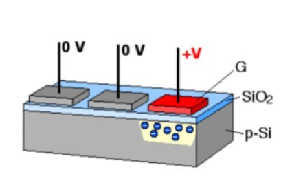
In the gate electrode, applying a positive voltage will generate potential well and collect the charge packet in it. You only need to apply a positive voltage in the correct order to conduct the charge pocket.

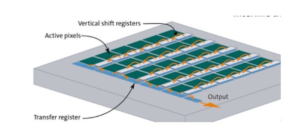
In a CCD for photosensitive use, there is a photosensitive region and a sensor area made of shift registers.
The image is projected on a column of capacitors through lenses, resulting in each capacitor accumulating a certain charge, and the number of charges is proportional to the incident light intensity there. A one-dimensional capacitive array for wire scanning cameras can scan a single layer of capacitors at a time, while a two-dimensional capacitive array for cameras and ordinary cameras can scan images projected on a focal plane. Once the capacitor array is exposed, a control loop will allow each capacitor to transfer its charge to the adjacent next capacitor. The charge in the last capacitor in the array will be transmitted to a charge amplifier and converted into a voltage signal. By repeating this process, the control loop can convert the charge in the whole array into a series of voltage signals. In digital circuits, these signals are sampled and digitized, usually stored; In analog circuits, they are processed into a continuous analog signal.
Conclusion
In a circuit, a CCD works by transferring electrical charges from one area to another. This is done by applying a voltage across an electrode, which causes the charge to move from one area to another. The movement of the charge is then measured and converted into a digital signal.
About Semco – Semco University is an educational website that is catering to the needs of students and researchers. Offering information on Lithium-ion batteries. The resources and content are compiled from various sources including manufacturers, test labs, crowdsourcing, etc. Our motto is to provide a viable resource for companies, students, and enthusiasts interested in participating in the Li-ion Battery industry. Our initiative is to make people aware of the benefits, and opportunities of the revolutionary Lithium Batteries for multiple applications.
For More Updates Follow Us
WhatsApp – Facebook – Instagram – Twitter – LinkedIn – YouTube


